Quantum Dot Arrays - Generating targeted nanostructure modulation
Ref.-No. 5639
Keywords: Production of quantum dots, modulation of nanostructures, calibration of molecular beam epitaxy (MBE), quantum photonics and optoelectronics
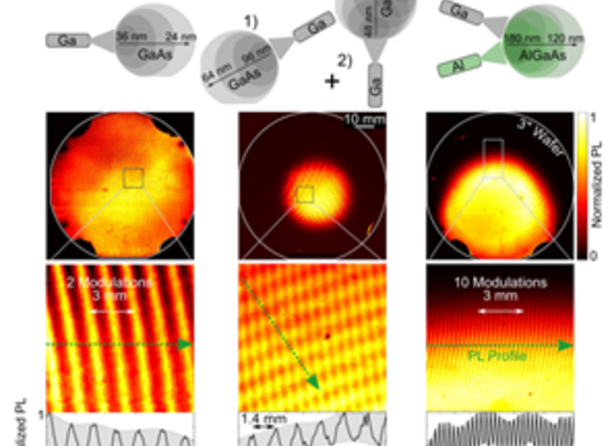
When developing novel devices based on semiconductor quantum dots (QDs), especially in quantum photonics/optoelectronics, it is essential to be able to precisely control their properties. The goal is to produce a specific QD density across the entire wafer area using conventional molecular beam epitaxy (MBE) without reducing QD quality. An invention by Ruhr University Bochum has just achieved this desired result. It is based on a new method that allows QDs to spatially arrange themselves on a substrate in a controlled manner. The method takes advantage of the fact that the self-organizing formation of nanostructures using MBE can be greatly influenced by a minimal modification of the substrate surface. This is accomplished first by using MBE to also generate a modulation of subnanoscopically rough and smooth surfaces on the substrate through a targeted vapor deposition gradient that can be adjusted, e.g., by a slight tipping. The QDs then form without further modification to the system or the growth conditions, creating a modulated surface density.
Competitive Advantages
- Opens the door to new optoelectronic components
- Suitable for molecular beam epitaxy (MBE) calibration
- Uses established manufacturing methods
- Targeted nanostructure generation on crystal edges
Commercial Opportunities
While nanostructures are suitable for the manufacture of optoelectronic components, manufacturing them is expensive. Their value, however, is enormous: Mode profiles can be created that “attract” lasers or densities for single-quantum dot applications such as single-photon sources can be calibrated directly. This allows for the expansion of the usable areas for quantum applications. One possible application of the invention is for the manufacturers of MBE systems to easily use this method to characterize the effusion cells and the structure itself with ultra-precision. This would be a decisive advantage for cell design and the usability of the resulting layers. Modulation also improves the yield on a single water: Instead of just a small area with a usable QD density, the entire wafer is used.
Current Status
Development is slated to continue as part of a DFG project, with the focus being on improving the method and the measuring technique.
An array with a periodicity in the submillimeter range was recently achieved; the array can also be functionally implemented with other quantum objects. A patent has been filed with the EPO under EP19177713.5. We are offering interested companies the opportunity to license and continue to develop this technology with the inventors at the university.
Relevant Puclications
The most significant results have been released in Nature Communications. Bart, N., Dangel, C., Zajac, P. et al. Wafer-scale epitaxial modulation of quantum dot density. Nat Commun 13, 1633 (2022). doi.org/10.1038/s41467-022-29116-8.
—
An invention of Ruhr University Bochum.


