Future Display Technology - Large Area Planar Lightguide
Ref.-Nr. 4659
Keywords: Displays, waveguide, electro-optic material, light emission, thin film technology, AMOLEDs
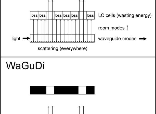
The presented technology is a two dimensional optical waveguide with very low attenuation. Incident light can be collected over the whole surface and propagate along the plane. The technology can be used for a new type of display. Light can be outcoupled from the waveguide at specific pixels. In conventional displays most of the light generated by the backlight gets absorbed by the LCD stack and color filters. Only a small portion of this light becomes visible from the outside. Thus the energy consumption of the backlight is very high. With the new technology, all of the light could be used, because it is distributed over the waveguide and released only where it is needed. The scientific background of this invention is a light scattering film in the node of a planar waveguide mode. Here the scattering film is invisible for propagating modes unless the waveguide is detuned. This way the node position is changed and the corresponding pixel area emits the light of the waveguide. As the pixels that are switched off collect ambient light, the display brightness adjusts according to the ambience. Even more important, the ability to efficiently extract light from a low-loss waveguide is expected to be a game changer for displays.
Vorteile
- Low loss planar waveguide and light collector in one device
- Enables displays with very low energy consumption and high contrast ratio
- Light is collected in the dark parts of an image and released only in the bright parts.
- No loss of backlight brightness like in conventional LCDs
- Very fast switching speed
- Technology can also be used as large scale light concentrator for photovoltaic power generation
Kommerzielle Anwendung
Battery runtime is a key feature for any mobile application. In smartphones and tablets most of the energy is needed for the illumination of the large display. The presented technology can be used to dramatically reduce the energy consumption of displays and to improve the readability in bright sunlight. It would also enable faster switching and a smaller building height. Another application would be a light concentrator for photovoltaic power generation. Sunlight can be collected on a square meter scale and only small stripes of high quality pv cells would be needed at the edges of the plane to convert the concentrated light to electricity. Both applications are located in a fast growing and high potential marked. Laboratory tests have already proven the advantages of the fundamental technology and further improvement is currently under development. PROvendis offers licenses for this invention to interested companies on behalf of the University of Wuppertal, Germany.
Aktueller Stand
Two international patent applications for this technology have been filed and are already published as WO2016000728A1 and WO2018086727A1. A further detailed description of the invention and scientific results can be provided to interested companies on request.
—
Eine Erfindung der Bergische Universität Wuppertal.


